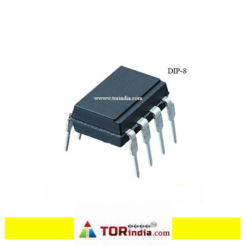
High Voltage Operation: Capable of driving high-side MOSFETs or IGBTs with voltages up to 500V (or 600V)High Speed: Designed for fast switching, with propagation delays matched for high-frequency applications. Typical rise and fall times are 25 ns and 17 ns respectively.Independent High/Low Side Channels: Provides separate output channels for both high-side and low-side gate driving, suitable for half-bridge and full-bridge configurations.Floating Channel for Bootstrap Operation: The high-side channel can be driven using a bootstrap circuit, enabling it to operate at high voltages.Wide Gate Drive Supply Range: Operates with a gate drive supply voltage from 10V to 20V. The logic supply range is 3.3V to 20V.Undervoltage Lockout (UVLO): Includes protection for both high-side and low-side channels, disabling outputs if the supply voltage is too low.3.3V Logic Compatible Inputs: Logic inputs are compatible with standard CMOS or LSTTL outputs, down to 3.3V logic levels.High Pulse Current Output: Output drivers feature a high pulse current buffer stage designed for minimum driver cross-conduction. Peak output current is 2A, with some sources citing 2.5A.Matched Propagation Delay: Propagation delays are matched to simplify use in high-frequency applications.CMOS Schmitt-Triggered Inputs with Pull-Down: Inputs are robust and suitable for noisy environments.Proprietary HVIC and Latch Immune CMOS Technologies: These technologies enable ruggedized monolithic construction.Thermal Shutdown Protection: Includes thermal shutdown protection to prevent overheating.Operating Temperature Range: Operates over a temperature range of -40°C to +125°C. Some sources indicate -40°C to +150°C.